Low-Power Sensing System of VEGF Concentration for Cancer Diagnosis

We developed a monolithic low-power sensing system for early cancer detection. The system uses a CMOS MEMS capacitive transducer with a gold interdigitated electrode (IDE) and DNA aptamers to sense the concentration of vascular endothelial growth factor (VEGF). When the DNA aptamer is immobilized with the VEGF sensor, it generates an electric double-layer capacitance. A two-step time-to-digital converter (TDC) is utilized. The proposed subsampling (SS) technique provides a higher conversion gain to reject noise interference and overcome the increase in noise floor introduced from the decoder due to lower supply voltage. The system is fabricated in TSMC 0.35-μm MEMS CMOS process with electroplated gold. Measurement results show that the power consumption of the readout circuit and the overall system is only 18 and 60.65 μW, respectively. The proposed system improves jitter by 49% and achieves 0.725-mV/pg-mL sensitivity.

Data Converter for Ultrasound Sound (US) Systems

CMOS capacitive micromachined ultrasonic transducer (CMUT) with integrated front-end circuits for portable high resolution ultrasonic imaging systems is presented. The CMUT array operates with 30 V power supply. In addition, the interlayer metal CMUTs with non-uniform membrane are proposed to improve the sensitivity in this paper. A prototype chip containing 48 elements as 12 channels is implemented. The conversion efficiency of the proposed CMUTs is 5.84 times higher than that in the published literatures.The maximum ultrasonic signal bandwidth is 4.5 MHz. CMUT array and the transimpedance amplifiers are integrated on the same chip. 

A 12-bit continuous-time ΔΣ modulator was designed and fabricated in 0.18-μm standard CMOS process. The chips size are 1.84 and 0.177 mm2 , and the total power consumption in the receiving mode is approximately 3.01 mW with 1.8 V power supply.


Teng-Chuan Cheng and Tsung-Heng Tsai, “CMOS ultrasonic receiver with on-chip analog-to-digital front end for high-resolution ultrasound imaging systems,” IEEE Sensors Journal, vol. 16, no. 20, pp. 7454-7463, Oct. 2016.

指叉擴展型CMOS MEMS壓力感測系統

本作品使用互補式金氧半導體微機電系統(CMOS-MEMS)製作平台完成將感測元件與讀取電路整合設計於單晶片上,做為無線顱內壓力感測系統植入的裝置。無線顱內壓力感測系統包含接收端(Reader)與傳輸端(Transponder),前者提供能量並且進行資料的讀取;後者將被植入於腦內偵測顱內壓力並於接受能量後傳輸資料,本研究之 MEMS 電容式感測器與電容數位轉換器(Capacitance to Digital Converter, CDC)整合於單一晶片,植入腦部測得顱內壓力資訊並於數位化後以無線傳輸至接收器後做後端處理。

在同樣的面積下,本作品採用3D的架構來增加電容的靈敏度,相比於原本傳統的電容可以有效縮小面積。同時我們針對腦壓訊號進行分析,評估腦壓在常態下所處的壓力值通常落在較小壓力範圍,因此我們根據此一特性採用了旁路切換邏輯控制,以減少類比數位轉換器之功率消耗。

Jyun-Jie Yang, Gordon Tsai, and Tsung-Heng Tsai, “A 53.36 pF/MPa CMOS-MEMS pressure sensor with compact size and integrated digital readout,” The 33rd IEEE International Conference on Micro Electro Mechanical Systems (MEMS), Jan. 18-22, 2020, Vancouver, Canada.

High-speed data converters

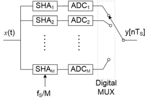
在特定製程下,單一通道類比數位轉換器的操作速度具有一定的限制,分時多工(Time-interleaving)架構常常被用於突破此限制,透過並行多個通道提高轉換器的整體操作速度。然而分時多工電路系統中,每個通道的電路可能存在相互不匹配,例如取樣放大器 (SHA)具有有限的帶寬,並且每個SHA的頻寬可能都不相同,將來各自通道的數位碼併在一起時將造成非線性失真。在這個作品中,我們提出了一種基於數位訊號處理的背景式校正技術,補償此類不匹配造成的誤差,改善高速類比數位轉換器的解析度。

Tsung-Heng Tsai, P. J. Hurst, and S. H. Lewis, “Bandwidth mismatch and its correction in time-interleaved analog-to-digital converters,” IEEE Transactions on Circuits and Systems-II, vol. 53, no. 10, pp. 1133-1137, Oct. 2006.

CMOS Pressure Sensor

A capacitive tactile sensor with high sensitivity is designed in CMOS MEMS process. A T-shaped protrusion is formed by the passivation layer to improve the linearity and sensitivity of the transducer. Moreover, high-resolution and high-sensitivity readout circuits are integrated with the MEMS transducer on the same chip to minimize the parasitic capacitance and noise.

鋰電池充電管理晶片

我們發表了一個使用人工智慧技術的鋰電池充電管理系統,包括快速充電器、電池老化診斷以及即時的充電狀態估計和平衡控制電路系統。充電器採用單電感單輸入雙輸出架構,實現電池模組之間的充電均衡。所提出的交錯式脈衝充電方式可以減少充電時間並減緩電池在充電過程中的老化現象。該方法還顯著抑制了電池單體溫度的上升,有利於實現充電平衡。在這個作品中,我們使用人工智慧神經網絡來檢測電池單元的健康狀態 (SOH) 並提高充電狀態 (SOC) 估計的準確性。晶片採用台積電 0.35-µm 製程實現。測量結果顯示交錯式脈衝充電可減少30%的電池溫度變化,在同時為四個電池單元充電時,可有效節省24%的充電時間,並實現了極低(僅 0.35%) 的 SOC 估計的平均絕對誤差。

Tsung-Wen Sun and Tsung-Heng Tsai*, “A Battery Management System Using Interleaved Pulse Charging with Charge and Temperature Balancing Based on NARX Network,” IEEE Transactions on Circuits and Systems I: Regular Papers, vol. 69, no. 4, pp. 1811-1819, Apr. 2022.


Lab. of Micro-Sensing & Systems

【Hiring! 歡迎加入實驗室!】

無論是工業4.0 或者是人工智慧(AI)系統,都仰賴大量收集資料(Big Data)用以訓練並建立系統模型。在感測網路中所需收集的資料十分微弱且多樣化,通常必須透過各式各樣的換能器(Transducer)將所要感測信號轉化為電信號,並經由類比數位轉換器(Analog-to-Digital Converter)轉成數位型式資料,方能由處理器或計算機進行運算。

我們研究的方向是設計低功耗感測器系統(Microsensing Systems),包括設計換能器於接收與反應因物理/化學變化造成之微小訊號、高靈敏度且低雜訊讀取電路、有線/無線資料傳輸通訊電路,大多數系統功能以CMOS製程完成整合設計。以生物感測系統為例,近年來已有許多公司投入新創研發,積極開發在照顧病患(或健康者)的當下,可以立即完成快速診斷測試之定點照護技術。發展的方向都是朝向疾病的提前預防和早期診斷,以及協助管理慢性病症。其中最為關鍵的技術就是將多種生物特徵的感測與分析功能整合設計到一個小型(便攜式)的裝置,方能提供個人化和預防性的醫療資訊。

於類比/混合訊號積體電路設計方面,透過晶片設計模擬、下線與量測,學生通常對感測系統能得到一定程度的理解,並針對整合系統所需之規格開發低功耗電路。較關鍵之電路設計技術包括(但不限於):

High-sensitivity CMOS MEMS transducers

Low-power analog front-end circuits

High-efficiency analog-to-digital converters

Energy harvesting/Power management systems

Low-power wireless communications

歡迎對IC設計感興趣的研究生/專題生加入實驗室。